Funding from the BMBFKnowledge Exchange Project Develops Measuring System to Produce Microchips
16 February 2024, by Newsroom editorial office

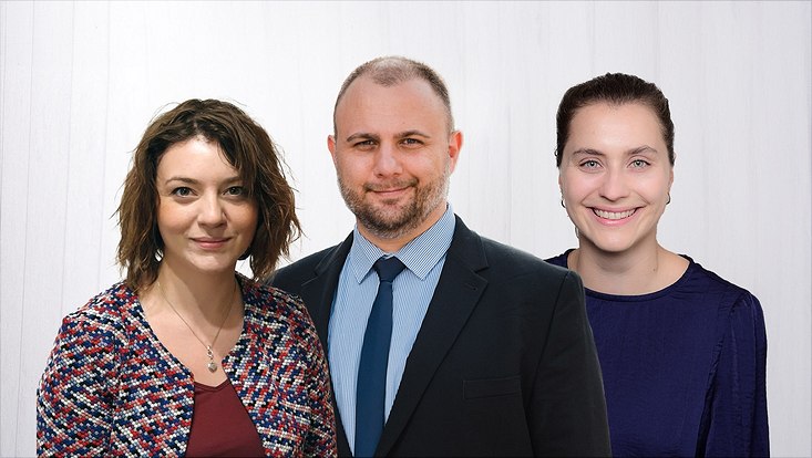
Photo: Heye Buss, CLASS 5 PHOTONICS GmbH
The University, DESY, and industrial partners are cooperating to achieve 1,000x greater throughput in the production of microchips. The Federal Ministry of Education and Research (BMBF) is now funding the development of a high-performance, extreme ultraviolet radiation source to the tune of €3.6 million.
Our connected, digital world will be fundamentally shaped by pioneering new technologies, including AI, 5G, virtual reality, and integrated cloud services. Even today there are an estimated 40 billion + connected end devices that increasingly rely on distributed computing power and data storage. In the next 10 years, this number will presumably rise sevenfold.
For the sake of energy and cost efficiency, it is crucial to further reduce the size of transistors and microchips. This can be done by implementing cutting-edge lithography—the production of microchips by transferring light patterns onto sensitive silicon plates (wafers)—using extreme ultraviolet radiation (EUV). This requires extreme precision and speed. Yet to date, there has been no system capable of measuring with the precision and speed required to verify mask and chip quality.
Therefore, MEGA-EUV, a new cooperative project between Universität Hamburg, DESY, the companies Class 5 Photonics and Amphos GmbH as well as other partners in the semiconductor industry will now focus on developing a high-performance, extreme ultraviolet radiation source. The goal is to demonstrate the world’s strongest coherent table-top EUV source at a wavelength of 13.5 nanometers. This should lead to a drastic increase in throughput when inspecting microchips created using EUV lithography.
This will involve innovative methods in cutting-edge high-performance laser technology. New approaches to generating EUV and imaging (Class 5 and Universität Hamburg) will be combined with high-performance Ytterbium-Innoslab lasers (Amphos) and systems for the post-compression of laser pulses (DESY). Promising fields of application are opening up in semiconductor production, material processing, and medical technology as well as in numerous scientific fields, for example, microscopy and ultra-fast optics.
“The principle of the new EUV source is based on fundamental work from over 30 years ago and for which a Nobel Prize in physics was awarded last year,” says Prof. Dr. Markus Drescher, who is coordinating the University’s part in the project. “I’m happy that we can once again show that persistence in basic research pays off for society.”
Dr. Bastian Manschwetus, project head responsible at Class 5 Photonics, explains: “We have had EUV sources in our product profile for a long time now but due to low output power their use was limited to scientific applications in materials research. With this project, we have found an ideal combination of brand leaders in the laser industry and outstanding research groups to strongly improve the performance of these kinds of light sources and make them available to a larger circle of users.”
The project is being funded within the scope of the Federal Ministry of Education and Research’s Neuartige photonische Werkzeuge für Wirtschaft und Gesellschaft—Laserbasierte Hochenergie-Strahlquellen program in the amount of €3.6 million. With this measure, the BMBF aims to support the transfer of innovative research findings in photonics, a key technology, thereby making important contributions to the fields of health, digitalization, and sustainability that are innovative, competitive, and address societal challenges.


